


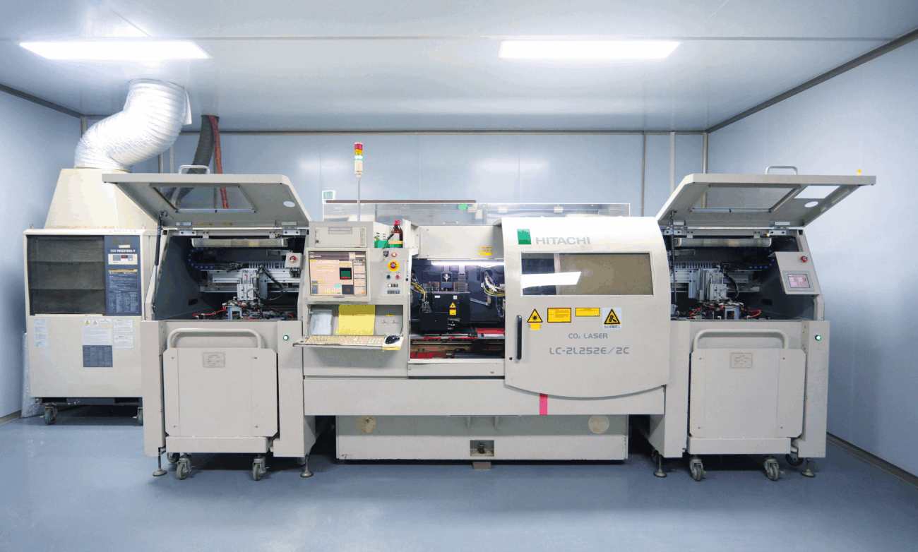
Laser drilling machine
Aperture range: 0.05-0.15 mm; positioning accuracy: ±5 μm
Copper-clad wire
Copper layer thickness: 0.3-0.5 μm; deposition rate: 0.1-0.2 μm/min; solution temperature: 25-35℃

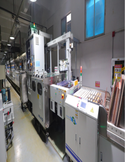
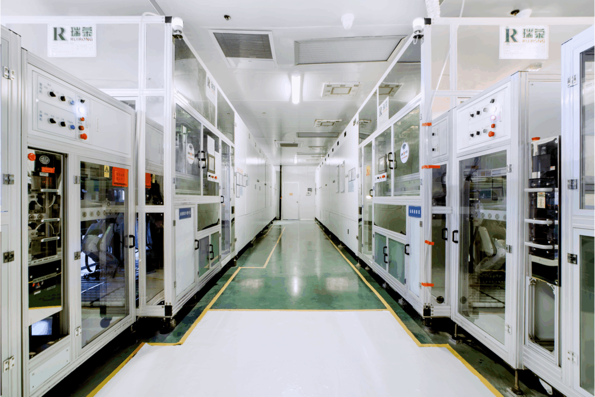
Pulse plating line
Current density: 2-10 ASF; Pulse frequency: 10-50 kHz; Deep plating capability: Copper layer thickness difference in holes ≤15%
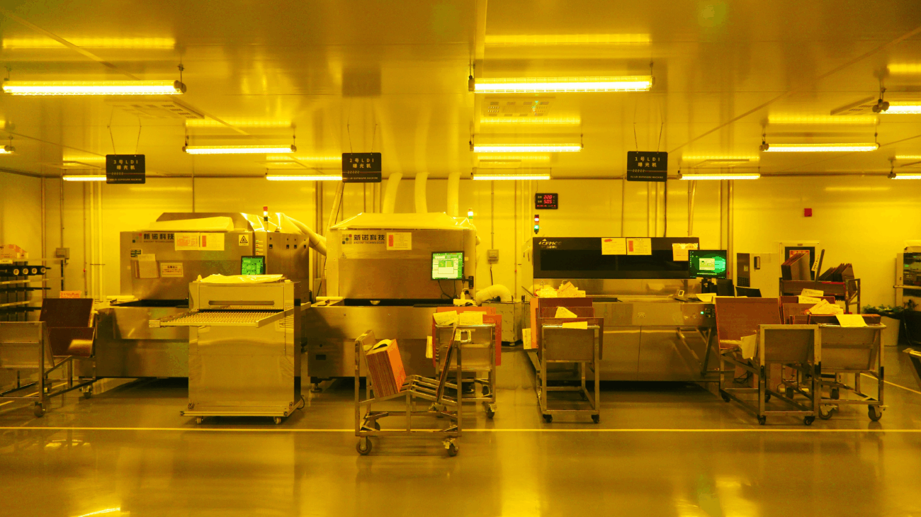
Laser Imaging Device (LDI)
Resolution: ≤10μm; Line width / pitch: ≤50μm/50μm; Registration accuracy: ±5μm
Vacuum lamination line
Pressure range: 2-5 MPa; Temperature control: ±1°C; Vacuum level: ≤10 mbar; Interlayer alignment accuracy: ±10 μm
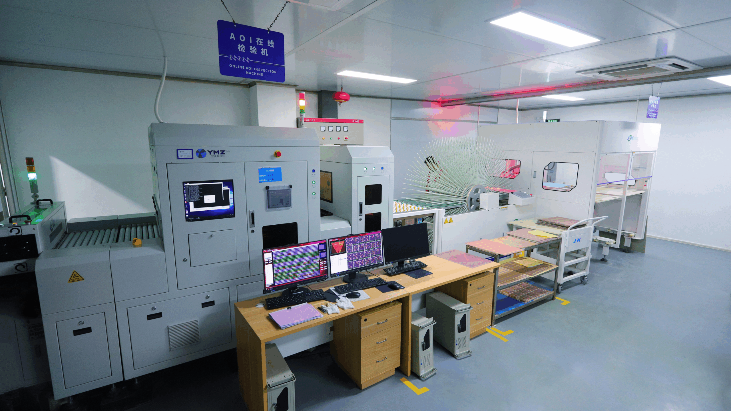
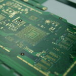
Fine etched lines
Etching rate: 1-3 μm/min; line width control accuracy: ±2 μm; undercut: ≤5 μm

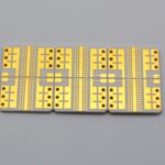
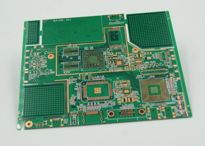
Ceramic PCB Board
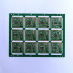
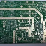
Double Sided PCB
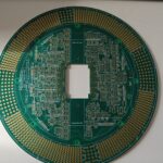
HDI Any Layer PCB
HDI PCB Board
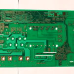
Heavy Copper PCB
IC Substrate PCBs
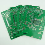
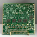
Multilayer PCB Board
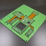
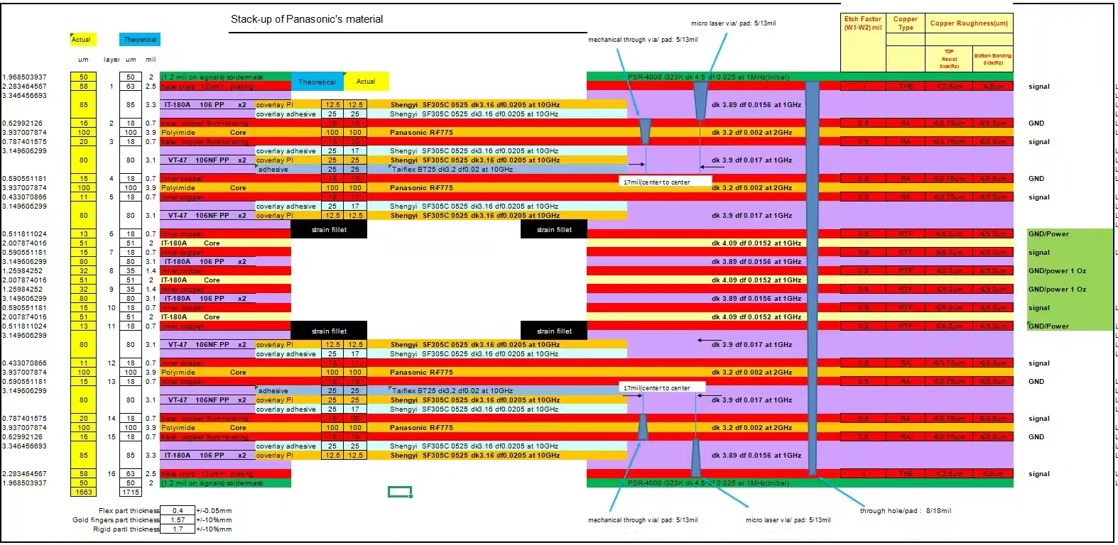
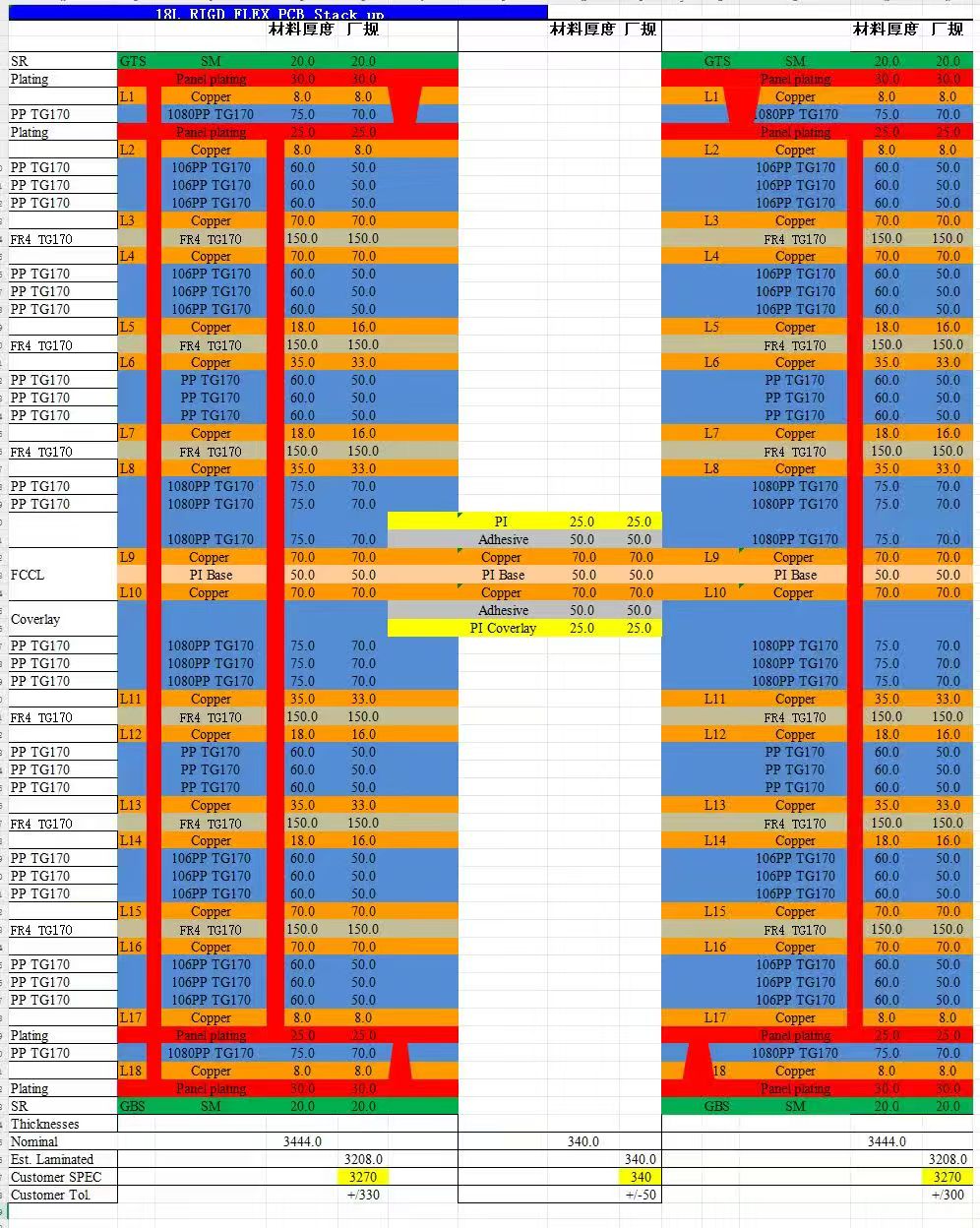
Rigid Flex PCB
Rogers PCB Board